Data Sheet
ADM4210
Rev. A | Page 5 of 16
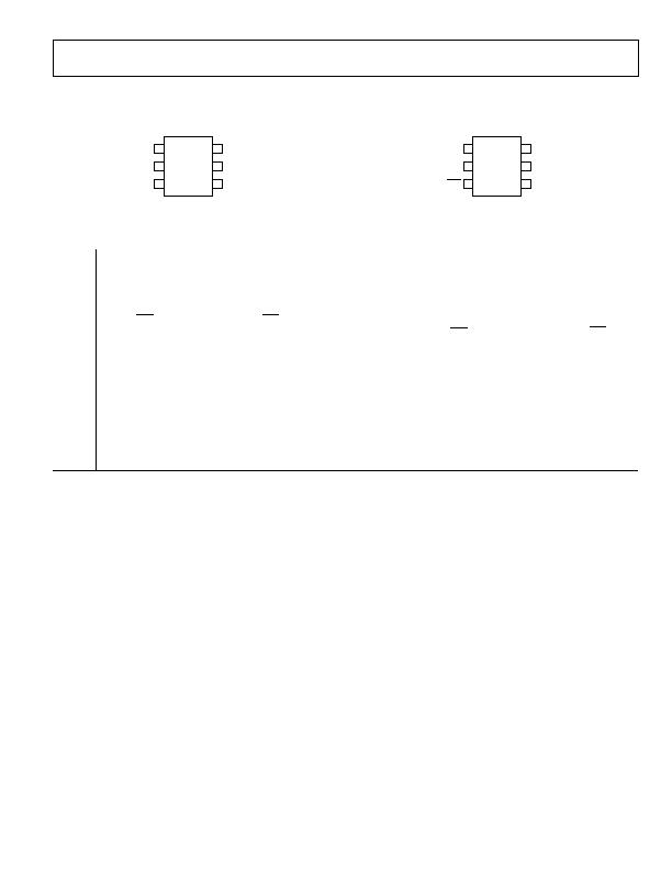
PIN CONFIGURATIONS AND FUNCTION DESCRIPTIONS
ON
IMER 1
GND 2
3
V
CC
6
GATE
4
SENSE
5
ADM4210-1AUJ
TOP VIEW
(Not to Scale)
Figure 3. Pin Configuration, 1AUJ Model
N-CLR
TIMER 1
GND 2
3
V
CC
6
GATE
4
SENSE
5
ADM4210-2AUJ
TOP VIEW
(Not to Scale)
Figure 4. Pin Configuration, 2AUJ Model
Table 4. Pin Function Descriptions
Pin No. Mnemonic Description
1
TIMER
Timer Input Pin. The initial and circuit breaker timing cycles are set by this external capacitor. The initial timing
delay is 272.9 ms/糉, and 21.7 ms/礔 for a circuit breaker delay. When the TIMER pin is pulled beyond the upper
threshold, the GATE turns off.
2
GND
Chip Ground Pin.
3
ON (ON-CLR
) Input Pin. The ON (ON-CLR
) pin is an input to a comparator that has a low-to-high threshold of 1.3 V with 80 mV
hysteresis and a glitch filter. The ADM4210 is reset when the ON (ON-CLR
) pin is low. When the ON (ON-
CLR
) pin is
high, the ADM4210 is enabled. A rising edge on this pin has the added function of clearing a fault and restarting
the device on the latched off model, the ADM4210-2.
4
GATE
Gate Output Pin. An internal charge pump provides a 12 礎 pull-up current to drive the gate of an N-channel
MOSFET. In an overcurrent condition, the ADM4210 controls the external FET to maintain a constant load
current.
5
SENSE
Current Limit Sense Input Pin. The current limit is set via a sense resistor between the V
CC
and SENSE pins. In an
overcurrent condition, the gate of the FET is controlled to maintain the SENSE voltage at 50 mV. When this limit is
reached, the TIMER circuit breaker mode is activated. The circuit breaker limit can be disabled by connecting the
VCC pin and SENSE pin together.
6
VCC
Positive Supply Input Pin. The ADM4210 operates between 2.7 V to 16.5 V. An undervoltage lockout (UVLO)
circuit with a glitch filter resets the ADM4210 when the supply voltage drops below the specified UVLO limit.
发布紧急采购,3分钟左右您将得到回复。
相关PDF资料
ADVFC32SH
IC CONV V/F F/V MONO TO100-10
FAN4800ASNY
IC CTLR COMBO PFC/PWM 16-DIP
FAN4800AUN
IC PWM/PFC CTLR COMBO 16-MDIP
FAN4800CUN
IC PWM/PFC CTLR COMBO 16-MDIP
FAN4802MY
IC PFC CTRLR AVERAGE CURR 16SOP
FAN4802SNY
IC CTLR PFC/PWM COMBO 16-PDIP
FAN6920MRMY
IC PWM CTLR PFC/QUASI-RES 16SOP
FAN6921MLMY
IC CTLR PFC/FLYBACK 16-SOICN
相关代理商/技术参数
ADM482EAR-REEL
制造商:Analog Devices 功能描述:QUAD SPDT ANALOG SWITCH 175 OHM CERDIP-16 (HOTS) - Tape and Reel
ADM483
制造商:AD 制造商全称:Analog Devices 功能描述:5 V Low Power, Slew-Rate Limited RS-485/RS-422 Transceiver
ADM483AR
制造商:Analog Devices 功能描述:Single Transmitter/Receiver RS-422/RS-485 8-Pin SOIC N
ADM483AR-REEL
制造商:AD 制造商全称:Analog Devices 功能描述:5 V Low Power, Slew-Rate Limited RS-485/RS-422 Transceiver
ADM483AR-REEL7
制造商:AD 制造商全称:Analog Devices 功能描述:5 V Low Power, Slew-Rate Limited RS-485/RS-422 Transceiver
ADM483ARZ
功能描述:IC TXRX RS485/RS422 LP 8SOIC RoHS:是 类别:集成电路 (IC) >> 接口 - 驱动器,接收器,收发器 系列:- 标准包装:1 系列:- 类型:线路收发器 驱动器/接收器数:5/3 规程:RS232 电源电压:3 V ~ 5.5 V 安装类型:表面贴装 封装/外壳:28-SOIC(0.295",7.50mm 宽) 供应商设备封装:28-SOIC 包装:Digi-Reel® 产品目录页面:918 (CN2011-ZH PDF) 其它名称:296-25096-6
ADM483E
制造商:AD 制造商全称:Analog Devices 功能描述:+-15 kV ESD Protected, EMC Compliant Slew Rate Limited, EIA RS-485 Transceiver
ADM483EAN
功能描述:IC TX/RX RS-485 LO-SLEW 5V 8DIP RoHS:否 类别:集成电路 (IC) >> 接口 - 驱动器,接收器,收发器 系列:- 标准包装:27 系列:- 类型:收发器 驱动器/接收器数:3/3 规程:RS232,RS485 电源电压:4.75 V ~ 5.25 V 安装类型:表面贴装 封装/外壳:28-SOIC(0.295",7.50mm 宽) 供应商设备封装:28-SOIC 包装:管件